 Outsourcing topic
 |
- Project outsourcing
- cost
control
- intellectual
properties protection
Customer
Service
center |
 TEL:(+86)-21-60514130
Email:yq@yqpcb.com
Address:Room.619,Building
1,No.333,JinGang Road, Shanghai, China
Zip:201206
|
Techno-article |
 PCB Design
Technology
PCB Design
Technology
PCB EMC Design
Relation of Copper Foil Thickness、 Line width、 Current
PCB ESD
Design
PCB
Check List
PCB Power Design
PSPICE Uses
PCB Impedance
Control
PCB Quality
Control
|
 My position: Homepage
Shanghai
YanQing Electronics Technology Co. ,Ltd, as a Professional PCB
design and service provider,
combining
our strategic partners, experienced project management team, and the
best designers, specializes in providing complete solutions for your PCB needs
;
Our services include schematic design, PCB Layout, Signal
integrity analysis, EMC consultation, templet manufacture&weld and
techno-support.
Our goal is to provide our clients high value by Best Quality
and Quickest solutions

|
|
 Our
services Our
services
 |
 High speed, High
density PCB Design High speed, High
density PCB Design
signal integrity
analysis
EMC
Consultation
PCB layout
engineers training
Library management
PCB templet
manufacture, weld
DFM/DFT
Integration
"Routing
Only" services available |
 Our team
 All of our engineers have 6+ years'
experience
All of our engineers have 6+ years'
experience
Partner with global industrial leaders, first class technical and
management platform employed
Carried on trains
by foreign expert for a long time
Maintains communion
with the internal expert
Experts at
complex, dense, PCB design.
Software--Cadence/allegro, PADS, Protel
Design capability
| High speed signal:10G CML GE/FE SATA LVDS... |
Max design layers :30
layers
|
| Max connections:25939 |
Max PIN count:35851 |
| Min via:8MIL(4MIL laser holes) |
Max BGA:BGA1932_45x45 |
| Min BGA PIN spacing:0.5mm |
Min line spacing:4MIL |
| Min line width:3.5MIL |
Max board area:508mm*432mm |
Services and Products
Data communication series:VOIP,xDSL, Ethernet switchboard, cut-in server
Optical network products: SDH, DWDM, METRO
Wireless products: GSM/GPRS, CDMA, WCDMA, base facilities
Multi-media products: video telephone, meeting TV,VOD
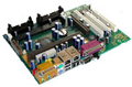
Computer products: services
MB, Notebook MB ,PC MB etc...
Consumable:DVD,MP4,Digital
Camera etc...
Control plate: Various
series of control plate
Various series of IC test

|